

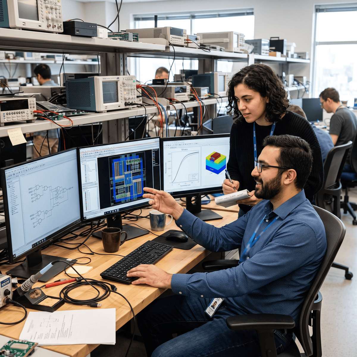
From chip architecture to timing closure, semiconductor design depends on simulation. CAE, TCAD, and EDA are three interconnected stages, each answering a specific design question. This course walks you through the workflow: how process recipes feed device simulations, which generate compact models for circuit timing analysis. You’ll learn to interpret simulation outputs across process-voltage-temperature corners, understand why margins matter, and recognize where process changes cascade to timing risk.
Whether you’re supporting a design team, managing process technology, or advancing your semiconductor foundations, this course demystifies the simulation ecosystem. By the end of this course, you will be able to: – Differentiate CAE, TCAD, and EDA stages by describing the design questions each answers – Trace the data flow from process recipe through TCAD to SPICE circuit verification – Interpret simulation outputs to explain how process changes affect circuit delay across corner models Basic semiconductor physics (transistor structure, doping) and familiarity with circuit concepts (voltage, current). No CAD tool experience required: every activity supplies pre-run simulation output for interpretation rather than asking learners to operate a simulator.
